ASIC System on Chip VLSI
VLSI has been in trend since it has arrived in the Market. VLSI stands for Very Large Scale Integration. It is basically a process of integrating thousands of transistors and ICs into a single chip. As the development of complex semiconductor and communication technologies increased over the years the development and need for Integration also started to increase. Before VLSI, most ICs had limited functions. VLSI lets IC designers add all of the functions that an electronic device has into one chip. A VLSI device that we all are familiar with is the microcontroller. Earlier integrated circuits used to contain only a few transistors. That time digital circuits also had only tens of transistors, along with a few logic gates and ICs had around two transistors. Since then, the number of transistors that an IC contains has increased.
System on Chip (SoC) v/s System in Package (SiP):
For Embedded Systems, SoCs are used on a very large scale. SOC is an IC which integrates all the components of electronic devices or systems onto a single chip. It may contain digital and analog signals and often mixed or radio frequency functions all on single chip. For a particular application whenever it is not possible to construct a SOC, an alternative option is system in package. SIP contains no. of chips in one package. For example, a SIP can have several chips such as DRAM, specialized processor, flash memory integrated with passive components such as resistors and capacitors and all of these components are mounted on a silicon substrate. This means that the entire components which form the functional unit can be built in a single multichip package. SOCs have become more common in the mobile computing market because of its low power consumption. For example, Microprocessor typically hasless than 100kB of RAM and often really has single chip system. SOC is typically used for more powerful processors and high performance devices like in case of smartphones.
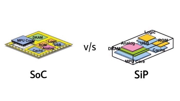
System-in-package (SiP) has created new challenges for set of design. SiP designs are only attempted or kept as an alternative when a barrier is reached such as constraints for size or performance and conventional system-on-chip (SoC) solutions are usually too expensive to be implemented. SiP has higher integration capacity which reduces the number of components in the system and also reduces the size and routing complexity of the PCB. However, SiP designs also have some challenges due to the dearth of similar design infrastructure between semiconductor technologies and the abundance of layout possibilities. The Packaging concepts include flip-chip stacked on-chip, chip stacked on-chip, chips placed side by side in a package and more concepts like this. The design partitioning process gets complicated because of all these.
ASIC:
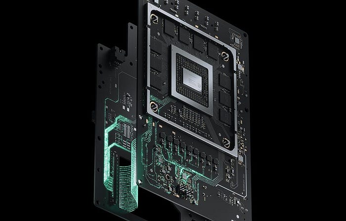
Application specific integrated circuit (ASIC) is typically a microchip which is designed for a special application. ASICs have different designs which allow specific actions to be performed inside of a particular device. Gate-array and full-custom design are the two primary design methods in ASICs.
As feature sizes of chips are shrinking and design tools are improving over the years, the maximum complexity which is possible in an ASIC has extended from 1,000 logic gates to over hundreds of millions logic gates. Modern ASICs include entire set of microprocessors, memory blocks which might include ROM, RAM, flash memory, EEPROM and many more larger building blocks. This type of ASIC is known as SoC (system-on-chip). To describe the functionality of ASICs, designers of digital ASICs use a hardware description language (HDL), such as System Verilog or VHDL. Nowadays Field-programmable gate arrays (FPGA) are the used as a technology for building a breadboard or prototype from standard equipments. Programmable logic blocks and Programmable interconnects allow the same FPGA to be used in many different applications. FPGAs are more cost effective than an ASIC design or even in production for systems having smaller designs or lower production volumes. The NRE (non-recurring engineering) cost of an ASIC can range up to the millions of dollars. Hence, device manufacturers usually prefer FPGAs for prototyping and devices which have low production volume and ASICs for very large production volumes. An example of ASIC can be Satellite-on-a-chip. It is an idea of building a completely functional satellite system as a monolithic integrated circuit which is able to be launched into space to perform a space mission while having a communication with the ground station.
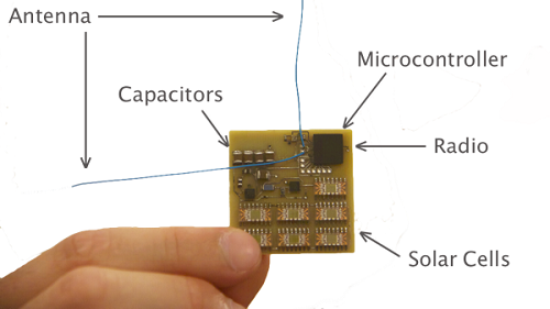
ASIC System on chip VLSI
The Design of ASIC is ever-changing and ever-challenging. The key factors amongst long-existing challenges are high cost, compact deadlines, complexity in design and verification of the designed product. As the Technology has shrunk from 180nm to 7nm the complexity increases.
According to Moore’s law, the transistors in a dense integrated circuit are double about every two years to search for more computational power and capacity.
Changes are required in design tools, strategies, and software and hardware capabilities in order to fulfill futuristic demands of chip designing. For such changes, ASIC design flow has been acquired for designing efficiently structured ASIC chip architecture and focus on its design functionalities.
ASIC Design FLOW:
The ASIC flow is divided into two parts: Front-end and backend. Front-end includes RTL designing with the help of System Verilog language to the circuit design which is called as Design synthesis.
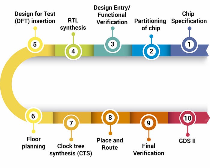
Various steps in the ASIC design flow are:
1. Chip Specification:
At this stage engineers define features, micro architecture, functionalities, and specifications with design guidelines of ASIC.
2. Design Entry / Functional Verification
Functional verification confirms the functionality and logical behavior of the circuit by simulation on a design entry level. This is often the stage where the look team and verification team acquire the cycle to come up with RTL code using test-benches which is understood as behavioral simulation. RTL code could be a set of code that checks whether the RTL implementation meets the planning verification.
3. RTL block synthesis
Once the RTL code and test bench are generated, the RTL team works on RTL description. They translate the RTL code into a gate-level net list employing a logical synthesis tool that meets required timing constraints. Thereafter, a synthesized database of the ASIC design is formed within the system.
4. Chip Partitioning
This is the stage during which the engineer follows the ASIC design layout requirement and specification to make its structure using EDA tools and proven methodologies. This design structure goes to be verified with the assistance of HLL programming languages like C++ or System C. Once all the functional blocks are implemented within the architectural document, the engineers must brainstorm ASIC design partitioning by reusing IPs from previous projects and procuring them from other parties.
5. Design for Test (DFT) Insertion
With the continued trend of lower technology nodes, there’s a rise in system-on-chip variations like size, threshold voltage and wire resistance. Thanks to these factors, new models and techniques are introduced to high-quality testing. SIC design is complex enough at different stages of the look cycle. Design for test is introduced with a listing of techniques:
Scan path insertion: A technique of linking all registers elements into one long register (scanpath).
Memory BIST (built-in Self-Test): MBIST may be a device which is employed to test RAMs. It’s a comprehensive solution to memory testing errors and self-repair proficiencies.
ATPG (automatic test pattern generation): ATPG could be a method of making test vectors / sequential input patterns to test the planning for faults generated within various elements of a circuit.
6. Floor planning (blueprint of chip)
In physical design, the primary step in RTL-to-GDSII design is floorplanning. It’s the method of placing blocks within the chip. It includes block placement, design portioning, pin placement, and power optimization. Floor plan determines the scale of the chip, places the gates and connects them with wires. While connecting, engineers be sure of wire length, and functionality which can ensure signals won’t interfere with nearby elements. In the end, simulate the ultimate plan with post-layout verification process.
7. Placement
Placement is that the process of placing standard cells in row. Various factors, just like the timing requirement, the web lengths and hence the connections of cells, power dissipation should be taken care. It removes timing violation.
8. Clock tree synthesis
Clock tree synthesis could be a process of building the clock tree and meeting the defined timing, area and power requirements. It helps in providing the clock connection to the clock pin of a sequential element within the required time and area, with low power consumption.
9. Routing
Global Routing calculates estimated values for every net by the delays of fan-out of wire. it’s mainly divided into line routing and maze routing. so as to form this ASIC design routable, placement density range must be followed. Placement density analysis is a vital parameter to urge better outcomes with less number of iterations.
10. Final Verification (Physical Verification and Timing)
After routing, ASIC design layout undergoes three steps of physical verification, called signoff checks. This stage helps to test whether the layout working the way it absolutely was designed to.
11. GDS II — Graphical Data Stream Information Interchange
In the last stage of the tape out, the engineer performs wafer processing, packaging, testing, verification and delivery to the physical IC. GDSII is that the file produced and utilized by the semiconductor foundries to fabricate the silicon and handled to client.
Significance:
SoC is truly a mix of ASIC, including full-custom and semi-custom (standard cells), reusable holding (IP) blocks (also called macro, hard macro, cores). IP core based design approach mainly intended for reducing design complexity and time to promote. Bus-based architectures like IBM core-connect, Motorola IP-bus, ARM’s advanced micro controller bus architecture (AMBA) that facilitates core-based SoC design.
The increase in density happens through multiple developments. A number of which are:
- Reduces the dimensions of circuits
- Reduces the effective cost of the devices
- Increases the operating speed of circuits
- Requires less power than discrete components
- Higher reliability
- Occupies a comparatively smaller area
Applications:
The area of applications of ASICs is extremely wide as they’re basically used everywhere where there’s a requirement for performance, customization and size. A number of the common categories of application are:
- Sensors and Transducers
- Laptop and Smartphone Processors
- Automotive and Avionic Components
- Satellite, Radar and related Communication processors
- Microprocessors, Memories, Micro controllers
Conclusion:
In a nutshell, an Application Specific Integrated Circuit or just an ASIC is defined as a circuit which is customized for a selected application instead of using it for general purpose. The main difference between standard ICs and ASICs is that the designer of the ASIC can directly be the customer who might need a clearer idea of the applying. ASICs has influenced the entire ecosystem of the semiconductor design and manufacturing like system design, fabrication and manufacturing process, testing and packaging and also the CAD tools. As user interactions with the machines are becoming higher and higher in number so the demand for the better system support is also increasing. It becomes a powerful engine to develop modern SoCs in industry to outpace the competition in performance, cost, and time-to-market. In the coming future, SoCs will be more useful in complex and advanced applications.
Hope You enjoyed this article!! Thanks for taking time to read. Be Kind and share happiness all around. It costs nothing to do that!
Have a wonderful day!